HDL Works

- Home
- Products
- Sales
- Support
- Company
- HDL Corner
HDL Works

Buttons with images and other graphical user interface elements will follow the scale size set in Windows and Linux.
In the User preference dialog, Application page, you can specify a font size increase, which will increase all font sizes for application text, for which you cannot select the font and size in the preference options (like in menus, dialogs and tab labels).

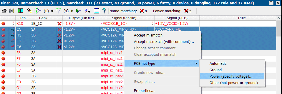
The context menu of the pin view has been simplified. The ‘Accept name mismatch’ and ‘Accept power mismatch’ entries have been merged in ‘Accept mismatch’. The item 'Change accept comment' has been added to change comment on a user accepted mismatch.
The items ‘Set/unset PCB net as a ground net…’, ‘Specify PCB voltage…’ and ‘Clear PCB voltage’ are moved in to the sub-menu ‘PCB net type’. Automatic is the default and should be used to remove the ground net of PCB voltage setting. Use ‘Other’ to force a net which was recognized as either ground or power net to be a regular user IO net.
The netlist type of a net can be set on any net. In the past power a voltage value could only be set on a net connected to a FPGA power pin. If a PCB net is manually marked as being a ground net we will now show this in the pin view by adding ' (-> GND)' to the name.
A new dialog to quickly edit groups of signals in the Signal view using regular expressions has been added for the signal view. This function is useful to change signals imported from the PCB with pre- of suffixes which need to be removed or changed.
Select the signals you want to change in the Signal view and choose 'Rename signals...' from the context menu.

The device view now shows pin labels for QFP packages.
Pins which are reserved, but different than do-not-use (like RSVDGND from Xilinx) show an R symbol.
Pins which can be both configuration and user IO have a diamond symbol inside the boundary.
The following changes have been made in the FPGA - PCB verification:
The ‘Accept power mismatch’ and ‘Accept name mismatch’ functionalities have been merged into a single ‘Accept mismatch’ function.
FPGA Control pin verification:
FPGA ground pin verification:
FPGA power pin verification:
The above options can be set (independently) in the Pin view matching and project verify options, and verify wizard dialog.

The ‘Clear unused PCB net types‘ is only enabled when it can be set and is used to removed voltage and ground settings on nets which are no longer present in the netlist.
Fabrication netlist format IPC-D-356 (often present with the Gerber data) has been added. The netlist type of a net (power, ground, normal) can be set on any net. In the past power (with a voltage value) could only be set on a net connected to a FPGA power pin.
If a PCB net is manually marked as being a ground net we will now show this in the pin view by adding ' (-> GND)' to the name.
Added the bank number to the tables ‘Pin list by severity’ and ‘List by FPGA pin’. Replaced fixed font sizes by ‘em’ and improved header. Replaced named anchors by ‘id’ attributes.
The dialog to wire non-FPGA symbols in Cadence Allegro (Tcl command Ioc::SchematicCsvDlg) has been extended with a ‘Column for the port’ entry. It allows you to use a specific port for a signal. When it is set the ‘Ports options’ entry is ignored. The ports used need to be present in the Allegro SKILL configuration file.
Copyright © 2004 - 2025 HDL Works